From atoms to systems: Prof Mario Lanza’s push to reinvent the electronics of the future
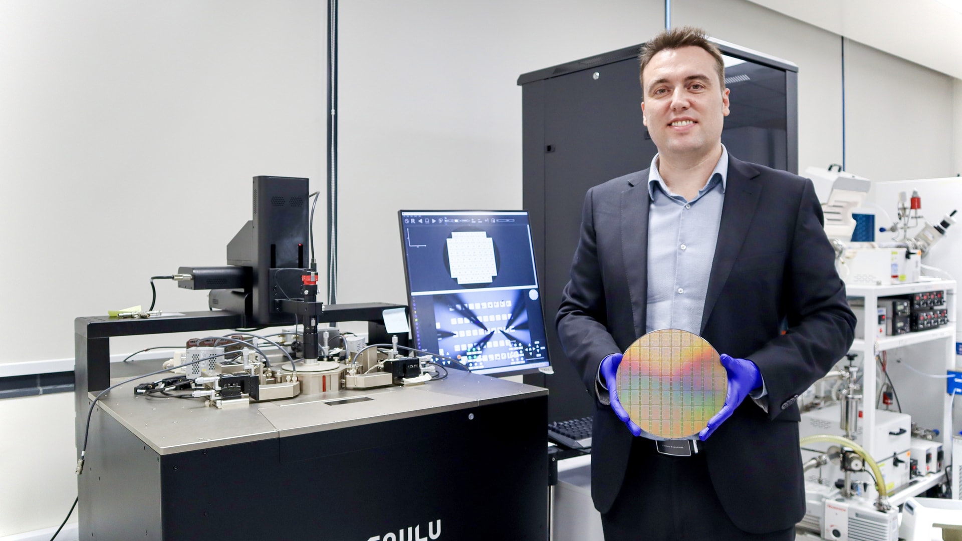
As electronic devices become smaller and more powerful, some of the biggest challenges facing engineers are playing out at almost unimaginably tiny scales. For Professor Mario Lanza, these challenges are an opportunity to rethink how electronics are designed.
Prof Lanza and group members from the Department of Materials Science and Engineering in the College of Design and Engineering (CDE) at NUS, are exploring new materials and device concepts that could help overcome the physical limits of conventional electronics. His recent studies and startup company show the breadth of this work — from understanding materials at the smallest one-atom limit to deploying them into tiny switches that make future wireless technologies more compact and energy-efficient.
At the heart of both is a deceptively simple idea: when electronics become extremely small, details that once seemed insignificant can transform how a device behaves.
Advanced nanoelectronic metrology
Understanding charge transport in novel materials with nanometric spatial resolution is critical in many branches of science, technology and engineering, and it has become a fundamental pillar in the field of semiconductors. This is a domain in which Prof Lanza’s team has been producing cutting-edge knowledge over the past decade.
For example, in a study published in Nature Materials on 1 July 2026, Prof Lanza’s team uncovers new fundamental physics that could shape how future electronics are designed. The paper’s first author is Dr Yue Yuan, who worked with Prof Lanza and the research team to investigate how atomically thin materials behave inside electronic devices.
His team has been investigating two-dimensional (2D) materials, which can be only a single atomic layer thick. Their extraordinary thinness offers the possibility of building electronic components with performance and functionalities superior to those used today.
But shrinking electronics to this scale introduces new problems. Electrons can pass through barriers intended to stop them — a phenomenon called quantum tunneling that unnecessarily increases energy consumption and usually accelerates device failure.
Using a technique called conductive atomic force microscopy (or CAFM), the researchers clarified a long debate related to the magnitude of quantum tunneling through various 2D materials deposited on diverse substrates. They discovered that the material itself is only part of the story. Tiny gaps between an atom-thin material and its electrodes can change the distance electrons must travel and, in turn, dramatically affect charge transport.
“At this extremely small scale, we’ve shown that tiny physical gaps between electrodes can matter more than the material’s own ability to block electrical current,” Prof Lanza said.
This finding, which was only possible thanks to the high lateral resolution of CAFM, gives engineers critical information for designing more reliable atomically thin devices and could ultimately inform the development of smaller and more energy-efficient chips, memory technologies and other advanced electronics.
Read more about this study here.

Memristive microchips
Another pillar of Prof Lanza’s research is the design, fabrication, characterisation and simulation of memristive devices. Memristors can be understood as “resistors with memory”, that is, they can be programmed at different values depending on the history of electrical stresses applied. These devices are called to play a key role for applications related to information storage, computation, encryption, and telecommunication.
For example, in a study published in Nature on 8 July 2026, Prof Lanza’s team deployed 2D materials to mitigate a growing challenge in wireless technology: how to pack more functionality into chips without making them larger or more power-hungry. The paper’s first author is Dr Sebastian Pazos, a senior device engineer working with Prof Lanza.
Modern wireless systems need growing numbers of radio-frequency switches to direct and control signals. While a 2G system used about four such switches in its signal-sending and receiving unit, 5G and future 6G systems may require 50 to more than 100 — potentially increasing the size, cost and power consumption of wireless hardware.
Prof Lanza’s team developed a radically smaller alternative using memristors. Based on hexagonal boron nitride (or hBN), an insulating 2D layered material, each switching element measures just two by two micrometres. Unlike conventional switches that typically require continuous power to maintain their state, these “memristive” switches retain their state after power is removed.
Crucially, the researchers did not demonstrate the technology only as a standalone laboratory device. They integrated the switches directly onto commercially manufactured gallium nitride (GaN) microchips and used them in working circuits that could adjust signal strength, redirect signals and select different frequencies.
The potential impact extends from smartphones and mobile networks to self-driving cars — technologies that will increasingly need to handle more wireless functions without simply becoming larger or consuming more power.
Read more about this study here.
Reinventing the transistor for AI
The third direction in which Prof Lanza’s team is making impact is on the design of hardware for artificial intelligence (AI). In another Nature article published in 2025, his team demonstrated that with only one standard silicon transistor, one can emulate both neural and synaptic behaviours. This is something that was thought to be impossible: engineers normally need dozens of transistors and bulky capacitors for each neural and synaptic block.
This groundbreaking discovery could be used to build high-performance spiking neural networks (SNN), a novel computing architecture that is particularly interesting to deploy AI on battery-powered and energy-harvesting devices, such as drones, robots, and wearables (a field often referred to as “Edge AI”).
Building on this breakthrough, Prof Lanza and Dr Pazos founded Newmorphic, a startup company located at one-north, a 6.5-hectare startup site often referred to as Singapore’s "Silicon Valley". On 28 and 29 October, Newmorphic went on to compete in SLINGSHOT 2026, Singapore’s flagship deep-tech startup competition held during the Singapore Week of Innovation and Technology (SWITCH) 2026, and emerged as winner in the “Advanced Manufacturing and Industrial Systems” domain.
Selected from a global pool of over 5,100 applications across 148 countries and placing among the top 10 finalists overall, Newmorphic’s victory underscores the commercial impact of its cutting-edge technology.

Reliable innovation in semiconductors
Together, these achievements capture Prof Lanza’s approach to innovation: understand what happens when materials are pushed to their physical limits, then turn those insights into new ways of building electronics.
A characteristic feature of Prof Lanza’s approach to nanoelectronics research is his emphasis not only on innovation, but also reliability. “We always try to repeat the experiments multiple times, using biasing protocols as close as possible as those required by industrial applications. We also usually report yield, variability, reliability and stability,” Prof Lanza said.
Furthermore, in most studies, his team employs manufacturing processes compatible with semiconductor wafer production lines, meaning that what they fabricate in the lab can be relatively easily transferred to the commercial manufacturing process. “We want to take advantage of the rich semiconductor and start-up ecosystem of Singapore and contribute to the development of new technologies, especially in the field of artificial intelligence.”
By understanding, controlling and ultimately exploiting phenomena at the atomic scale, his work is helping lay the foundations for electronic technologies that could be smaller, smarter and more energy efficient.
Read more information about his team here.